Development of Laser Selective Plating Technology for Heterogeneous Integrated Substrates
EU Funded Project No. 10-085-P-0001 · R&D project 05-001 · August 2026 – August 2028
About the project
AKONEER, together with the State Research Institute Center for Physical Sciences and Technology (FTMC), is implementing the R&D project 05-001 “Development of Laser Selective Plating Technology for Heterogeneous Integrated Substrates”.
The R&D project is implemented under the Eureka Network Globalstars R&D call with Taiwan and forms part of the project “Increasing the Level of Internationalisation of Science through the Implementation of Eureka Network Activities-III” (Project No. 10-085-P-0001).
Project goal
To develop a new-generation multilayer glass-based integrated circuit (IC) substrate for advanced semiconductor packaging, with high interconnect density, low warpage and good high-frequency performance.
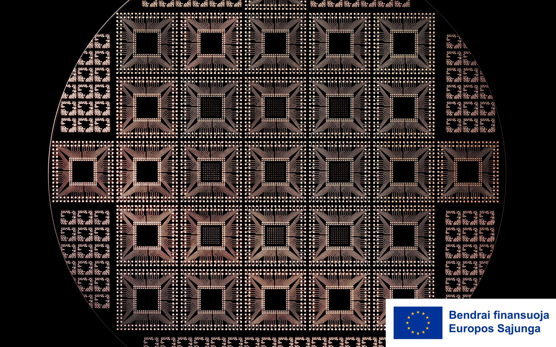
The core technology is SSAIL (Selective Surface Activation Induced by Laser), developed at FTMC. It forms 3–5 µm wide copper traces directly on glass without photomasks. Such substrates are needed for artificial intelligence, high-performance computing (HPC) and 5G/6G systems.
Planned activities
AKONEER
– Development of laser beam shaping and high-speed scanning methods for activation tracks of up to 5 µm width without damaging the substrate (together with FTMC).
– Design, assembly and calibration of a prototype laser beam delivery system integrating the laser source, beam-shaping optics and scanning.
FTMC (project coordinator)
– Optimisation of the SSAIL process on a polymer TBF layer.
– Chemical activation of through-glass vias and deposition of the copper seed layer.
– Development of electroless copper filling of the vias.
– Electrical and reliability testing of the multilayer glass substrate prototype.
Expected results
A tested multilayer glass substrate prototype (approx. 50 × 50 mm, 2–3 metallised layers) at technology readiness level TRL 7, and one patent application.
Funding

The project is funded by European Union funds, co-financing funds and the state budget of the Republic of Lithuania under progress measure No. 12-001-01-02-01 “Strengthening innovation ecosystems in science centres” of the Science Development Programme of the 2022–2030 Development Programme, managed by the Ministry of Education, Science and Sport of the Republic of Lithuania.
Project Information
| Project No. | 10-085-P-0001 | |
| Duration | 08/2026 - 08/2028 | |
| Value of the project | 302,206.86 EUR | |
| Project coordinator | State Research Institute for Physical Sciences and Technology (FTMC) | |
| Funding administered by | Research Council of Lithuania (LMT) |