SSAIL
High-resolution conductive traces can be formed on polymers, glass, ceramics, silicon and other dielectric materials. Trace width can go below 5 µm.
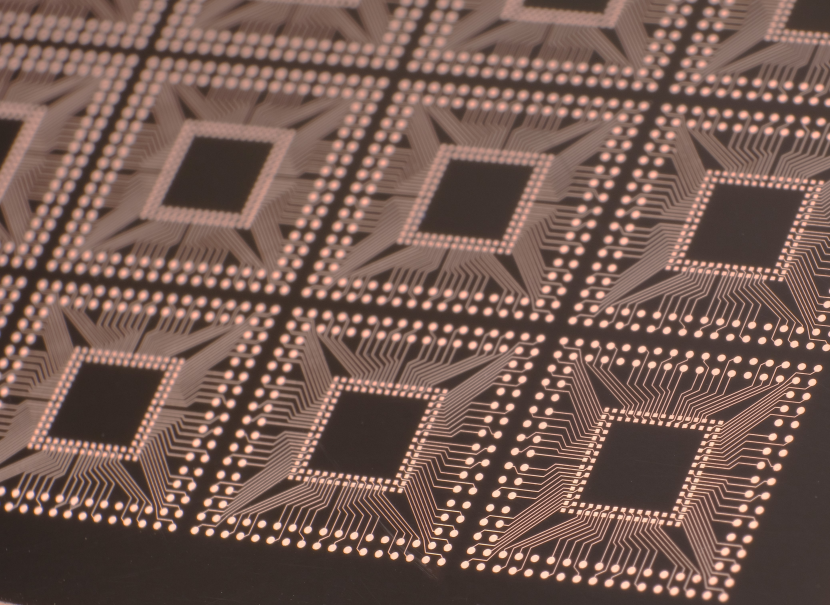
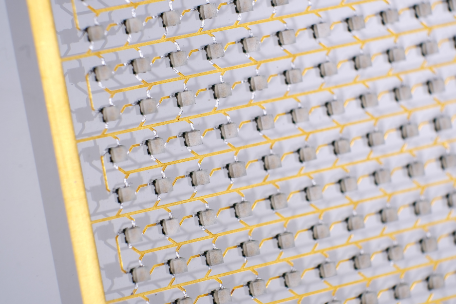
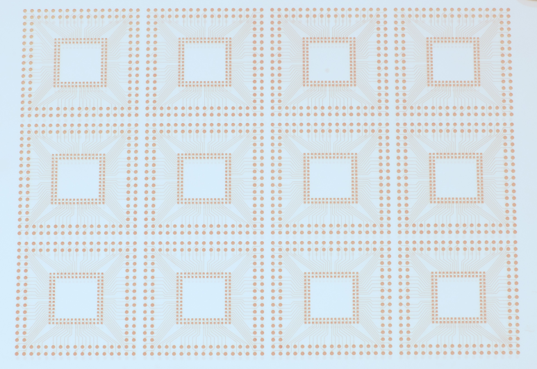
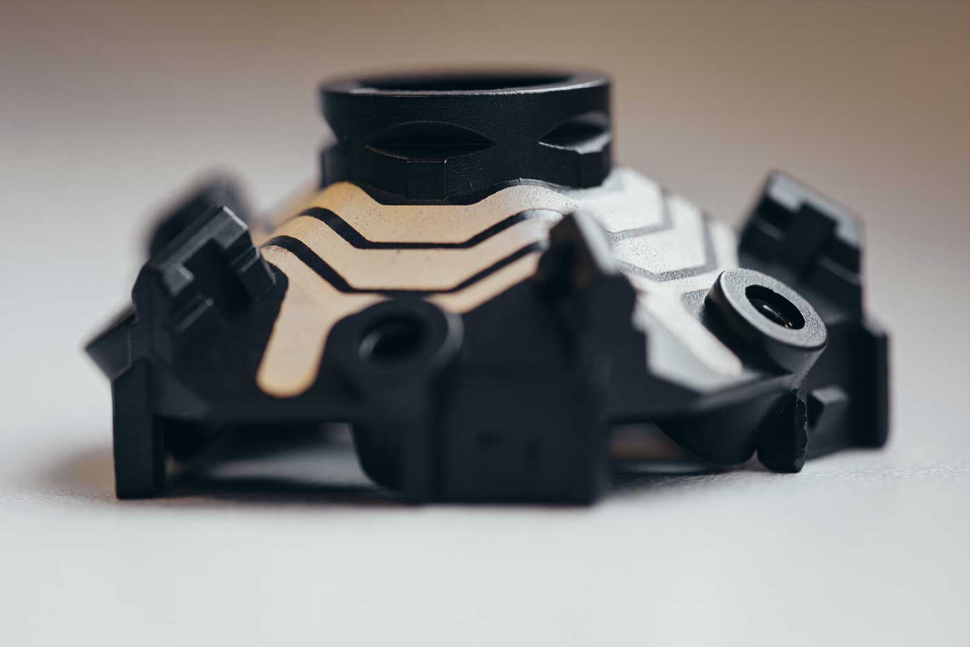
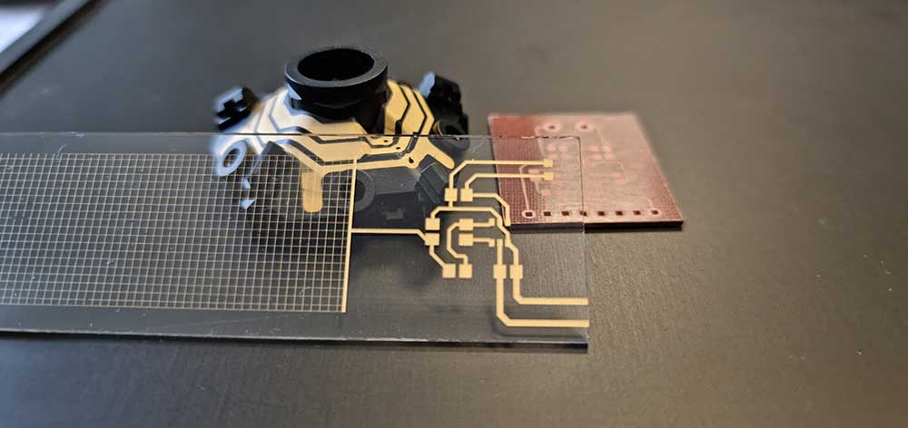
With a patented SSAIL technology conductive traces can be formed on many standard dielectric materials (polymers, ceramics, glass, silicon). It enables tighter electronics packaging on flat or 3D surfaces (with traces down to 1 µm width), making antennas directly on/in parts and creating functional surfaces.
SSAIL technology has several advantages over traditional methods for creating conductive traces. It eliminates the need for masks, costly lithographic processes, and specialized coatings, lowering manufacturing complexity and costs. The process is environmentally friendly because it reduces material waste and does not require the hazardous chemicals used in traditional etching techniques. Furthermore, SSAIL allows for direct integration of electronics into mechanical components, resulting in lighter, more compact, and more reliable electronic devices.
Another significant advantage is its adaptability to various shapes and materials, enabling the seamless integration of electronic functions into non-traditional substrates. This creates new opportunities for applications in consumer electronics, medical devices, automotive components, aerospace, and Internet of Things (IoT) devices. The ability to create highly precise, fine-pitch conductive traces on flexible, rigid, and 3D surfaces makes SSAIL an excellent choice for next-generation electronic designs.
HOW DOES IT WORK
SSAIL is a two-step process:
1. Laser activation of the surface for traces. It is done by scanning the surface with a laser beam.
2. After the laser activation, the part goes through a chemical process:
a) Chemical activation is done with a special solution, which prepares laser-activated areas for electroless plating.
b) Electroless plating with copper and passivation layers (nickel, silver, gold).
FLEXIBILITY OF SHAPES
Using SSAIL technology electrical traces can be used on different types of parts:
- 3D surfaces
- Thin films
- Flexible materials
- Through via plating
On most materials, a trace width of 15 µm can be achieved (down to 1 µm on some materials). Process speed depends on trace width and substrate material and can reach several hundreds of mm2/s.
MATERIALS
The technology works on many different dielectric materials. Some of the materials include:
| PC/ABS | PPS | Getinax |
| PA6 | PF | FR-4 |
| PVC | PI | Epoxy |
| PMMA | PC/ABS for 3D printing | RO3003™ Laminates |
| PET | PTFE | SITAL ceramic |
| PEEK | ABF | Al2O3 ceramic |
| PPA | PA4 | Glass (soda lime) |
| LCP | PBS | Fused Silica |
| PBT | PREP 200 | Silicon |