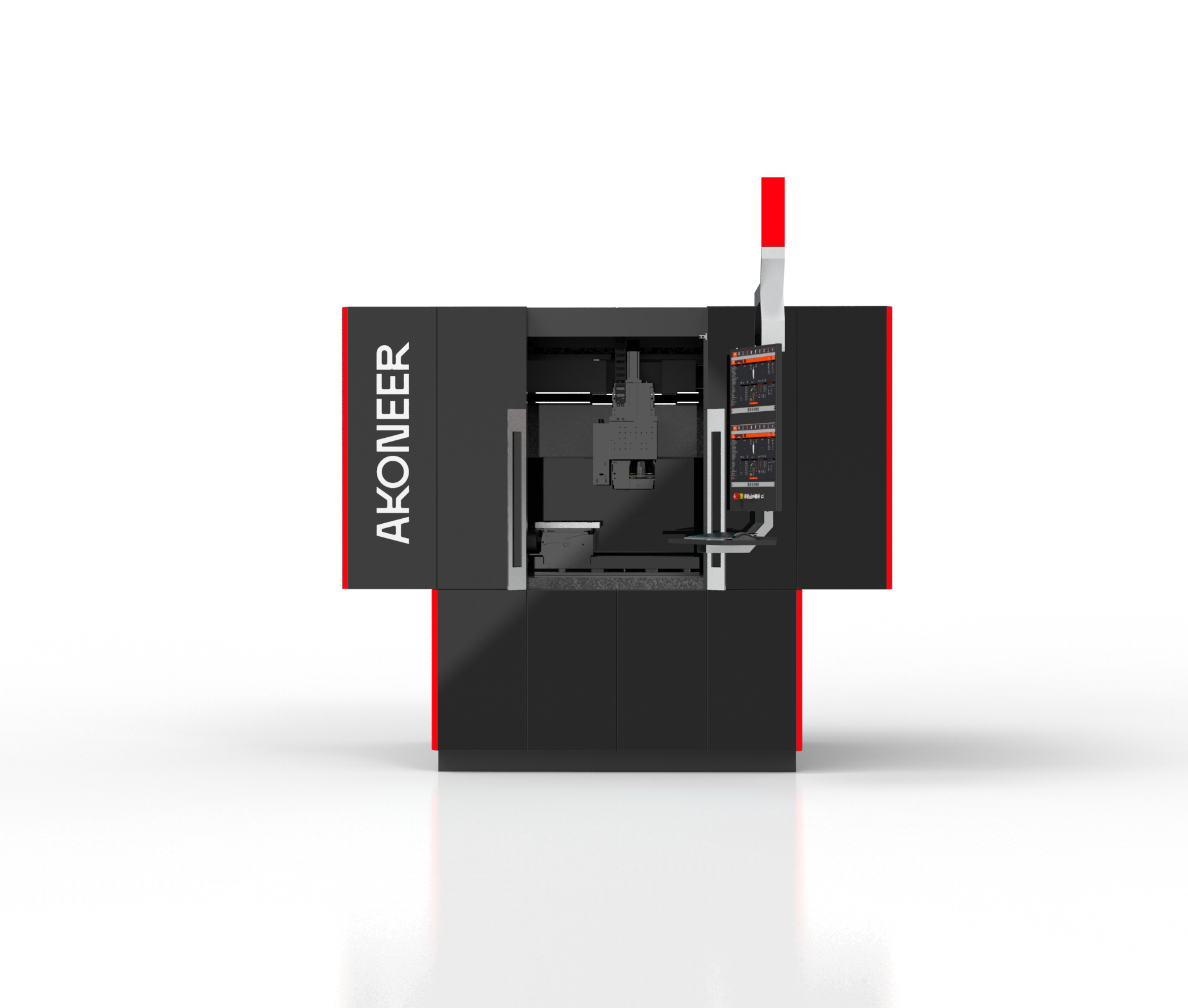
Laser marking silicon
Laser marking on silicon is a critical technology for inscribing detailed and durable information in the electronics and semiconductor industries.
Laser marking is a versatile technology used to inscribe information on various materials. Among these materials, silicon stands out due to its widespread use in the electronics and semiconductor industries. Silicon's unique properties make it an ideal substrate for laser marking, which offers precision, durability, and efficiency. This article delves into the process of laser marking silicon, its benefits, and its applications.
Understanding the laser marking process
Laser marking involves using a focused beam of light to alter the surface of a material. This can be achieved through techniques like engraving, annealing, or foaming, each producing distinct interactions between the laser and the material. For silicon, laser engraving is common, where the laser removes a small amount of material to create a permanent mark. Typically, lasers operate at powers ranging from 20 to 100 watts, with a precision repeatability of ±0.01 mm. The laser's parameters, such as power, speed, and wavelength, can be adjusted to achieve the desired depth and contrast. This flexibility allows for intricate designs, essential in the semiconductor industry.
Benefits of laser marking silicon
Laser marking silicon offers several advantages. It provides unmatched precision, allowing for detailed and complex patterns—a necessity in the semiconductor industry, where components are miniaturized and demand precise markings. It's a non-contact process, exerting no physical pressure on the silicon, thus preserving the integrity of wafers or chips. The marks are durable, resistant to wear and environmental factors, ensuring long-lasting traceability. Additionally, the process is efficient and easily automated, suitable for high-volume production environments. For example, Samsung utilizes laser marking on silicon wafers to enhance traceability, reducing error rates by over 15% in production.
Applications in the semiconductor industry
In the semiconductor industry, laser marking is used for marking silicon wafers, which serve as the foundation for semiconductor devices. Accurate marking is crucial for traceability and quality control. Laser marking inscribes alphanumeric codes, logos, or barcodes onto wafers, essential for tracking manufacturing processes, ensuring compliance with industry standards, and facilitating inventory management. Additionally, laser marking is crucial in producing microelectromechanical systems (MEMS), miniaturized devices combining electronic and mechanical components. The precision offered by laser marking is vital for creating intricate features required by MEMS technology.
Challenges and considerations
While laser marking silicon offers numerous benefits, challenges exist. Selecting appropriate laser parameters to achieve desired mark quality without damaging silicon is crucial. The laser's wavelength is significant, as silicon exhibits varying absorption properties at different wavelengths. Infrared lasers, such as fiber lasers, are commonly used due to their compatibility with silicon. Managing heat dissipation is another challenge; excessive heat can cause thermal damage, affecting semiconductor device performance. Careful control of the laser's energy and exposure time is essential. As technology advances and silicon components shrink, demand for higher precision in laser marking continues to grow.
Future trends in laser marking technology
The field of laser marking technology is constantly evolving, driven by advancements in laser sources, optics, and software. A promising trend is the development of ultrafast lasers, operating at extremely short pulse durations. These lasers offer enhanced precision and minimize thermal effects, ideal for delicate silicon structures. Another trend is integrating machine vision systems with laser marking equipment, allowing real-time monitoring and feedback for accurate alignment and mark quality. Additionally, the increasing adoption of Industry 4.0 principles leads to more interconnected and intelligent laser marking systems, facilitating seamless data exchange and improving overall efficiency.
In summary, laser marking silicon is a critical technology in the electronics and semiconductor industries. It provides precise and durable markings essential for traceability, quality control, and compliance. While challenges exist, ongoing advancements in laser technology pave the way for greater capabilities. As demand for high-performance and miniaturized semiconductor devices continues to rise, laser marking will remain a key enabler of innovation and progress in the industry.
