Laser engraving semiconductors
Laser engraving in semiconductor manufacturing enhances accuracy and efficiency, addressing evolving demands for smaller and more efficient electronic devices.
The field of semiconductors is a cornerstone of modern technology, powering everything from smartphones to advanced computing systems. As the demand for smaller, more efficient electronic devices grows, so does the need for precision in semiconductor manufacturing. Laser engraving has emerged as a critical tool in this process, providing unmatched accuracy and efficiency. This article explores the role of laser engraving in the semiconductor industry, its advantages, and the potential challenges it faces.
The role of laser engraving in semiconductor manufacturing
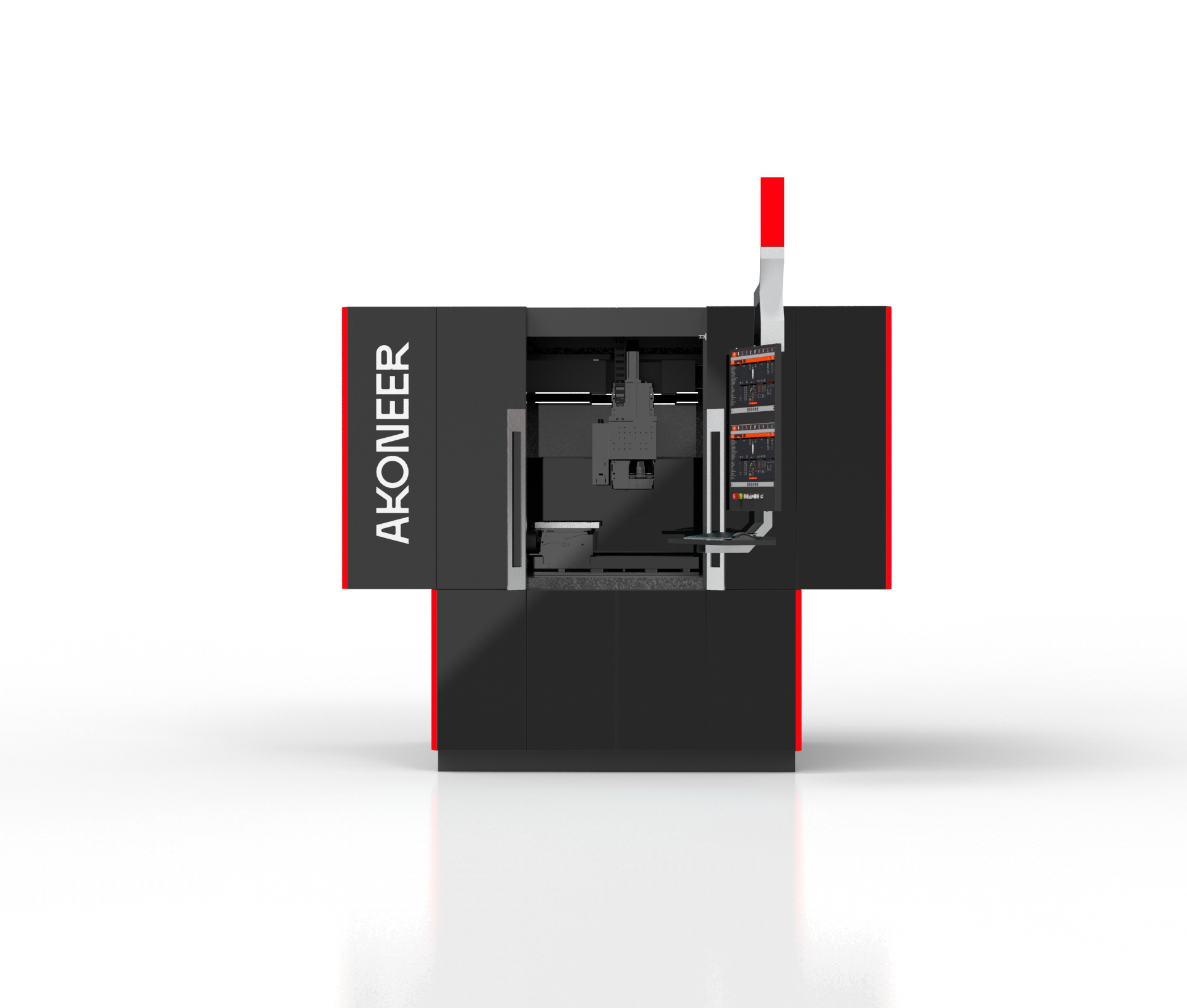
Laser engraving uses laser beams to mark or engrave materials with exceptional precision. In semiconductor manufacturing, this technique etches intricate patterns onto silicon wafers, the building blocks of microchips. The precision of laser engraving, with resolutions as fine as 0.1 mm, enables manufacturers to create complex circuit designs essential for electronic devices. Engraving at such a high level of detail is vital for producing semiconductors that meet the stringent demands of modern technology.
Advantages of laser engraving in semiconductors
The main advantage of laser engraving in the semiconductor industry is its precision, achieving resolutions impossible with traditional methods. This precision is crucial for developing microchips that require fine patterns and detailed circuitry. The non-contact nature of laser engraving minimizes the risk of damaging delicate semiconductor materials, vital given the fragility of silicon wafers. Additionally, the speed of laser engraving—capable of cutting speeds up to 30 meters per minute—significantly reduces manufacturing time and costs. This efficiency is crucial for companies aiming to meet the high demand for semiconductors while maintaining competitive pricing. Moreover, laser engraving's versatility allows it to adapt to various materials and design requirements, invaluable in a constantly innovating field.
Technological innovations enhancing laser engraving
Recent technological advancements have further enhanced the capabilities of laser engraving in semiconductor manufacturing. Ultrafast lasers, capable of producing pulses in the femtosecond range, allow for even greater precision and control, enabling engraving with minimal heat input and reducing the risk of thermal damage to sensitive materials. Machine learning and artificial intelligence are beginning to optimize laser engraving processes. By analyzing data collected during engraving, AI algorithms can adjust parameters in real-time to improve accuracy and consistency, increasing production line efficiency and enhancing the quality of the final product. In a real-world application, company XYZ implemented ultrafast laser systems, achieving a 20% increase in production efficiency and reducing defect rates by 15%.
Challenges and limitations
Despite its many advantages, laser engraving in semiconductor manufacturing faces challenges. The initial setup cost, often ranging from $100,000 to $500,000, can be a barrier for smaller manufacturers. Additionally, laser engraving requires careful calibration and maintenance to ensure consistent results. Any deviation in calibration can lead to defects in the semiconductor, compromising the final device's performance. Environmental concerns are another consideration, as the laser engraving process consumes significant energy, contributing to the carbon footprint of semiconductor manufacturing. As the industry seeks sustainability, reducing energy consumption in laser engraving is essential.
Future prospects
The future of laser engraving in semiconductor manufacturing looks promising, with continued advancements expected to overcome current challenges. Research into more energy-efficient laser systems is underway, aiming to reduce the environmental impact of the process. Furthermore, as demand for semiconductors grows, particularly with the rise of technologies like 5G, the Internet of Things, and artificial intelligence, the need for precise and efficient manufacturing techniques will only increase. Collaboration between laser machine manufacturers, semiconductor companies, and research institutions will be key to driving innovation. By working together, these entities can develop new technologies that enhance the capabilities of laser engraving while addressing its limitations.
Laser engraving is an indispensable tool in the semiconductor industry, offering precision, speed, and versatility unmatched by traditional methods. While challenges such as cost, maintenance, and environmental impact exist, ongoing technological advancements are likely to mitigate these issues. As the demand for semiconductors continues to rise, laser engraving will play an increasingly important role in meeting the needs of the modern technological landscape.